Samsung boosts HBM specialist hiring, scales back foundry recruitment

The company will halt experienced hiring in the second half for its loss-making System LSI unit

A researcher at a Samsung R&D center
Jeong-Soo Hwang 2
2025-08-13 16:42:14 hjs@hankyung.com
Korean chipmakers

Samsung Electronics Co. is stepping up recruitment of seasoned high-bandwidth memory (HBM) specialists in a push to reclaim leadership in the semiconductor industry, betting on a rebound after a weak second quarter

The hiring targets experienced engineers in next-generation semiconductor and chip packaging technologies, including hybrid bonding, a process seen as crucial for improving performance in artificial intelligence and other computing applications.

By contrast, the South Korean chipmaker is scaling back experienced hires in its underperforming foundry division compared with previous years, underscoring its focus on the HBM segment, where it lags behind local rival SK Hynix Inc.

According to Samsung Electronics on Tuesday, its Device Solutions (DS) division, which oversees the company’s semiconductor operations, plans to hire experienced professionals across six of its nine main business units.

The six units are the memory chip business, foundry, semiconductor research center, global manufacturing and infrastructure, test and system package and AI center.

Samsung will open applications for the second-half hiring through Aug. 19.

It declined to specify a target headcount. But industry observers expect hiring to be substantial, pointing to signs of recovery in the memory chip market. Samsung is forecasting a second-half earnings rebound, driven by HBM products.

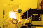
Samsung's 12-layer HBM3E samples (Courtesy of Samsung Electronics)

HBM

Specifically, Samsung is looking for package development experts with the ability to design new architectures for advanced HBM, while product planning hires will be tasked with liaising with clients interested in customized HBM.

Custom HBM refers to versions of the vertically-stacked DRAM product in which the base die -- the layer at the bottom, which functions as the chip’s brain – is equipped with features specified by the customer.

Samsung is expected to bring customized HBM to market as early as next year to narrow the gap with the HBM pioneer SK Hynix.

HYBRID BONDING

Samsung is making efforts to improve hybrid bonding technology, which eliminates the use of bumps – tiny connectors currently used to stack DRAM chips in HBM production – by directly linking chips to one another.

The technology is considered essential for manufacturing products with 16 or more DRAM layers as it can reduce the thickness of HBM stacks and lower heat generation.

The 12-layer HBM3E is the most advanced AI memory chip currently in mass production. SK Hynix became the world's first company to showcase a 16-layer HBM3E early this year.

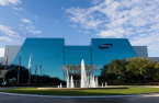
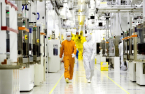
Samsung Electronics' Pyeongtaek Campus in Gyeonggi Province

Meanwhile, Samsung will halt experienced hiring for the System LSI business in the second half of this year.

The unit, which develops non-memory products such as its Exynos application processors and image sensors, extended its losses in the second quarter.

Along with the foundry division, the System LSI unit is among the main drags on Samsung's quarterly results.

Samsung's DS division reported 400 billion won ($288 million) in second-quarter operating profit – its lowest profit since a 2 trillion won operating loss in the fourth quarter of 2023.

Write to Jeong-Soo Hwang at hjs@hankyung.com
 

Yeonhee Kim edited this article.

Samsung to produce Apple’s next-gen chips at US foundry plant

Samsung to produce Apple’s next-gen chips at US foundry plant

Samsung's chip plant in Austin, Texas (Courtesy of Samsung Electronics)  The global memory chip powerhouse Samsung Electronics Co. will produce chips for Apple Inc. at its semiconductor manufacturing facilities in the US, a move expected to blunt the impact of Washington’s planned ta

Samsung eyes earnings recovery in H2 on higher HBM sales

Samsung eyes earnings recovery in H2 on higher HBM sales

Samsung Suwon Digital City (Courtesy of Samsung Electronics)  Samsung Electronics Co. expects its earnings to recover in the second half of this year, banking on rising demand for its premium high-bandwidth memory (HBM) chips and improved foundry performance after reporting poor second-qua

Samsung clinches $16.5 billion chipmaking deal from Tesla

Samsung clinches $16.5 billion chipmaking deal from Tesla

Samsung's foundry chip plant in Taylor, Texas (Courtesy of Samsung Electronics) Samsung Electronics Co., the world’s top memory chipmaker, has clinched a landmark contract chipmaking deal worth $16.5 billion from Tesla Inc., raising hopes of a turnaround for its underperforming foundry bu

S.Korea’s most prominent business leader returns with all charges cleared

S.Korea’s most prominent business leader returns with all charges cleared

Samsung Group Chairman Jay Y. Lee gives a speech during a visit by US President Joe Biden to the chipmaker's Pyeongtaek plant in 2022 After nearly a decade spent fighting allegations of corporate wrongdoing, Samsung Electronics Co. Chairman Lee Jae-yong has been acquitted on all charges of acco

Samsung on hiring spree to bolster US foundry sales

Samsung on hiring spree to bolster US foundry sales

Samsung Foundry Forum 2024 held in San Jose, California on June 12-13, 2024 Samsung Electronics Co. is on a hiring spree for senior sales managers in its foundry business, offering generous compensation packages, as it goes all-in to secure large contract chipmaking orders from US Big Tech firm

SK Hynix leads Samsung in customized HBM; lands Nvidia, Microsoft deals

SK Hynix leads Samsung in customized HBM; lands Nvidia, Microsoft deals

The exterior of SK Hynix's semiconductor plant in Icheon, Gyeonggi Province (Courtesy of Yonhap) SK Hynix Inc. has secured Nvidia Corp., Microsoft Corp. and Broadcom Inc. as key clients of its customized high-bandwidth memory (HBM), positioning the South Korean chipmaker at the forefront of bot

Ex-TSMC executive joins Samsung Foundry to lead US expansion

Ex-TSMC executive joins Samsung Foundry to lead US expansion

Samsung Electronics' chip cleanroom Samsung Electronics Co. has brought a former Taiwan Semiconductor Manufacturing Company Ltd. (TSMC) executive on board to lead its North American foundry operations, ramping up efforts to bolster its loss-making contract chipmaking business in the US. Earlier

Samsung’s system chip, foundry business under close scrutiny for overhaul

Samsung’s system chip, foundry business under close scrutiny for overhaul

A researcher in a Samsung Electronics chip cleanroom Samsung Electronics Co., the world’s largest memory chipmaker, has put its system chip and foundry businesses under tight scrutiny for a possible business overhaul, including an executive reshuffle and employee relocation, as it faces a

Samsung foundry ‘relief pitcher’ Han Jin-man vows to improve 2-nm yields

Samsung foundry ‘relief pitcher’ Han Jin-man vows to improve 2-nm yields

Han Jin-man, Samsung's new foundry chief Samsung Electronics Co.'s new contract chipmaking business chief said on Monday he will go all-in to improve the company’s advanced 2-nanometer chip processing technology and secure more clients to take on foundry rival Taiwan Semiconductor Manufac

Samsung to replace chiefs of 3 key posts: Memory, foundry, system LSI

Samsung to replace chiefs of 3 key posts: Memory, foundry, system LSI

A researcher in a Samsung Electronics chip clean room Samsung Electronics Co. plans to replace the three key posts of its semiconductor business — memory, foundry and system LSI — as the South Korean tech giant struggles to compete with its rivals, particularly in the booming AI chi

Samsung launches dedicated HBM, advanced chip packaging teams

Samsung launches dedicated HBM, advanced chip packaging teams

A researcher in a Samsung Electronics chip cleanroom Samsung Electronics Co., the world’s largest memory chipmaker, has officially launched a team dedicated to developing advanced high-bandwidth (HBM) memory, a core chip in powering artificial intelligence (AI) devices.The Suwon, South Ko

Samsung to build $281 million chip packaging R&D center in Yokohama

Samsung to build $281 million chip packaging R&D center in Yokohama

A researcher at a Samsung Electronics chip cleanroom South Korea’s Samsung Electronics Co., the world’s largest memory chipmaker, will build a 40 billion yen ($281 million) advanced chip packaging research and development center in Japan amid improving ties between the neighboring c

(* comment hide *}