Samsung to set up chip packaging R&D center in Yokohama, raise stakes vs TSMC
The company bought a building in Yokohama to turn it into a research lab
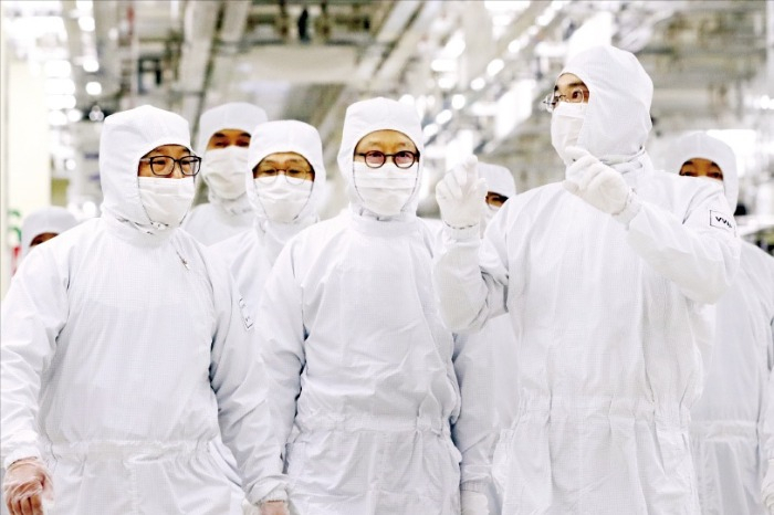
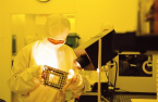
Samsung Electronics Chairman Lee Jae-yong (far right) inspects the semiconductor packaging line at the Samsung Cheonan Factory in Cheonan, Korea (Courtesy of Samsung)
Samsung Electronics Co. will set up an advanced chip packaging research and development center in Yokohama, Japan with an investment of 25 billion yen ($170 million), according to semiconductor industry sources on Wednesday, intensifying its rivalry with TSMC in the high-stakes packaging market.
The South Korean chipmaker expects the research lab, slated to open in March 2027, to bolster its collaboration with Japanese semiconductor material and equipment suppliers, including Disco Corp., Namics Corp. and Rasonac Corp., as well as the University of Tokyo.
The City of Yokohama, which in December 2023 announced Samsung’s plan to build an R&D center in the city, will provide a 2.5 billion yen subsidy for the launch of the research lab.
The Leaf Minato Mirai building, a retail property now converted into an R&D space, will house the lab and pilot production lines.
Samsung has purchased the building, located near an R&D hub within Yokohama’s Minato Mirai district, for an undisclosed sum.
The property measures a total floor area of 47,710 square meters with 12 floors above ground and four below.
It is Samsung’s first major building purchase in Japan in a decade, following the sale of a 57% stake in its Roppongi headquarters building in Tokyo in March 2015 as part of restructuring efforts.
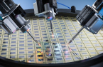
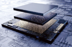
Advanced packaging is a technology that connects graphic processing units, high-bandwidth memory (HBM) and other memory chips so they function as a single chip.
It is considered a key process in manufacturing AI chips, enhancing their performance without having to shrink the nanometer through ultra-fine processing, which is technologically challenging.
For Samsung, packaging is a core element of its ambitious turn-key chip manufacturing services, which combines foundry and packaging – areas in which Taiwan Semiconductor Manufacturing Co. (TSMC) maintains a clear lead.
LOCAL TALENT HIRING
In 2019, the Taiwanese company similarly set up a research lab at the University of Tokyo to advance its packaging technologies.
Japan is home to key materials and equipment makers.
They include Rasonac and Namics, leaders in bonding film used to connect and support chips; Uemura Co., a specialist in gold-plating materials for packaging; Disco, a dicing equipment maker; and MEC Co., which focuses on adhesives and surface-treatment materials.
Samsung plans to hire a large number of researchers with master’s and doctoral degrees from the University of Tokyo, within a one-hour drive of its research facility in Yokohama.
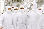
Samsung Electronics Chairman Lee Jae-yong (third from left) inspects the semiconductor packaging line at the Samsung Cheonan Factory in Cheonan, Korea (Courtesy of Samsung) AI chips go through several stages of production – design, foundry manufacturing, advanced packaging and testing.
Excluding design, dominated by fabless firms like Nvidia Corp. and Advanced Micro Devices Inc., Taiwan is seen as the leader in foundry, packaging and testing.
TSMC provides both foundry work and advanced packaging to integrate SK Hynix Inc.'s HBM with Nvidia Corp.’s graphics processing units for AI accelerators.
Its combined share of the foundry, packaging and testing market rose to 35.3% in the first quarter of 2025 from 29.4% a year earlier, according to Counterpoint Research.
Taiwan’s ASE Technology Holding, a traditional packaging powerhouse, ranked third in the field with a 6.2% share in the first quarter, behind Intel Corp.’s 6.5%.
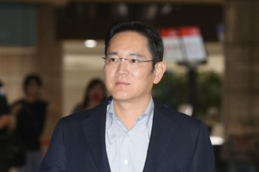
Samsung Electronics Chairman Lee Jae-yong, also known as Jay Y. Lee Samsung, the only South Korean company with a presence in the turn-key manufacturing field, holds a 5.9% share of the chip packaging market.
Its capacity and technology in 2.5D and 3D advanced packaging, which stack and arrange different chips vertically, still lag behind TSMC’s.
However, Samsung recently clinched a $16.5 billion foundry contract for Tesla’s next-generation AI6 chips, a deal industry observers attribute to Samsung’s enhanced turn-key service capabilities.
The advanced chip packaging market is projected to grow to $80 billion by 2032 from $34.5 billion in 2023, according to Counterpoint Research.
Write to Jeong-Soo Hwang, Chae-Yeon Kim and Ui-Myung Park at hjs@hankyung.com